Exact Expression for the Skin Effect (Including Surface Roughness)
This option adds an exact skin effect (which includes the effects of surface roughness) to metallic surfaces and/or wires.
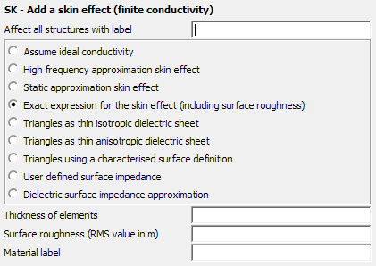
Figure 1. The SK - Add a skin effect (finite conductivity) dialog.
Note: The material parameters for the skin effect are defined with the DI card. The SK
card then uses the label defined at the DI card.
Parameters:
- Thickness of elements
- The thickness d of the surface elements in metres (if an SF card is present, this is always scaled).
- Surface roughness (RMS value in m)
- The surface roughness of the metal specified as a RMS value in m.
- Material label
- Label of the material which will be used (as specified in the DI card).
The required parameters are , and (defined with the DI card). If applied to surfaces then also the thickness d is required.
The following restrictions apply:
- A good conductivity is required, satisfying the condition .
- For wires with wire radius
the surface impedance is given
bywhere J0 and J1 are Bessel functions.
(1) - For a sheet of thickness, d, with properties
,
with
the wave propagation constant in the sheet
is given by
and the wave impedance in the sheet by
. The reflection coefficient at the interface
between the sheet and the environment is defined as
. The surface impedance is given by
(2)