SK Card
This card defines a skin effect, ohmic losses, dielectric sheet, characterised surface definition, arbitrary user defined impedance boundary condition on wire segments and surface elements or a dielectric surface impedance approximation. Layered dielectrics can also be defined.
In the Home tab, in the Define group, click
the ![]() Media icon. From
the drop-down list select the
Media icon. From
the drop-down list select the ![]() Losses (SK) icon.
Losses (SK) icon.

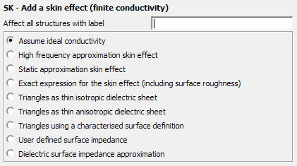
Figure 1. The SK - Add a skin effect (finite conductivity) dialog.
Parameters:
- Affect all structures with label
- The label to which the skin effect is applied is specified. All mesh elements with this label are assigned the skin effect.
- Assume ideal conductivity
- Ideal conductivity is assumed as if no SK card is specified for this label. All other parameters are ignored.
- High frequency approximation skin effect
- Apply the high frequency approximation skin effect to structures with the specified label.
- Static approximation skin effect
- Apply the static (ohmic losses) approximation skin effect to structures with the specified label.
- Exact expression for the skin effect (including surface roughness)
- Apply the exact expression for the skin effect (which includes the effects of surface roughness) to metallic surfaces and/or wires with the specified label.
- Triangles as thin isotropic dielectric sheet
- Treat metallic triangles with the specified label as thin isotropic dielectric layers (possibly consisting of multiple layers).
- Triangles as thin anisotropic dielectric sheet
- Treat metallic triangles with the specified label as thin anisotropic dielectric layers (possibly consisting of multiple layers).
- Triangles using a characterised surface definition
- Treat triangles with the specified label as a characterised surface (a surface defined by transmission and reflection coefficient data).
- User defined surface impedance
- Treat wire segments and surface elements with the specified label as an arbitrary user defined complex surface impedance.
- Dielectric surface impedance approximation
- Treat homogeneous dielectric regions in free space with the specified label as a dielectric surface impedance approximation.