Infinite Planes and Half-Spaces
Use an infinite plane or half-space to model a ground plane efficiently. The number of triangles in the model is reduced as the ground plane is not discretised into triangles.
On the Construct tab, in the Structures
group, click the ![]() Planes/arrays icon. From the drop-down list, select
Planes/arrays icon. From the drop-down list, select ![]() Plane / ground.
Plane / ground.
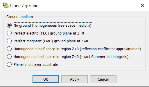
Figure 1. The Plane / ground dialog.
No Ground (Homogeneous Free Space Medium) [Default]
The model is solved in a homogeneous environment filled with free space medium. Edit the properties of free space if required.Infinite Homogeneous Half Space (Reflection Coefficient Approximation)
An infinite half space is added using the reflection coefficient ground plane approximation, where the reflected component is added to each field.Note:
- This method does not support conducting structures inside the ground.
- Structures may touch the ground plane, but may not cross the ground plane surface.
- Place conducting structures at least away from the ground plane.
- This technique is faster and less accurate than the exact Sommerfeld integrals method.
- Perfect electric (PEC)
- Add an infinite PEC ground plane at Z=0 (in the global coordinate system).
- Perfect electric (PMC)
- Add an infinite PMC ground plane at Z=0 (in the global coordinate system).
- Homogeneous half space in region Z<0 (reflection coefficient)
- Add an infinite dielectric or a metallic ground plane at Z=0 (in the global coordinate system).
Infinite Homogeneous Half Space (Exact Sommerfeld Integrals)
An infinite half space is added using the Sommerfeld integrals to solve the exact boundary condition with the appropriate Green's function.Note: This method supports
conducting structures inside the ground.
- Homogeneous half space in region Z<0 (exact Sommerfeld integrals)
- Add an infinite dielectric or a metallic ground plane at Z=0 (in the global coordinate system).
Planar Multilayer Substrate
Add an infinite planar multilayer substrate orthogonal to the Z axis (in the global coordinate system).Note:
- Supports arbitrarily shaped dielectric bodies inside the substrate.
- Enclose the substrate in a MoM / SEP region to create a planar multilayer substrate with finite size.