Planar Multilayer Substrate
With this option a multilayer dielectric substrate in the XY plane is taken into with the Green’s function.
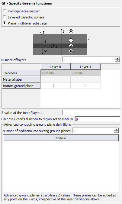
Figure 1. The GF - Specify Green's functions dialog, set to Planar multilayer substrate.

Figure 2. Example of a 4 layer substrate with a metallic ground plane
Parameters:
- Number of layers
- Number of layers in the substrate (layer 0 — the upper half-space) is not included in the number. As indicated in the figure of the card, layer 0 is the upper half-space, layer 1 is just beneath this, and so forth.
- Thickness
- Thickness of the layer (is scaled by the SF card).
- Material label
- Label of the material to be used for the layer (as defined in the DI card).
- Bottom ground plane
- By checking Bottom ground plane at the respective layer, a user can choose to have a ground plane at the bottom of the selected layer.
- Z-value at the top of layer 1
- The value of the Z coordinate at the transition between layer 0 and layer 1.
- Limit the Green’s function to region set to medium
- An optional parameter which allows for the planar multilayer substrate to be limited to a specified dielectric region. A dielectric medium must be defined and a dielectric region set to this medium. (Refer to the DI card and DL card for more information.) The planar multilayer substrate is then limited to this dielectric region specified by the label of the dielectric medium (as defined in the ME card). For more information refer to the combination of MoM/SEP and planar Green’s function in the CADFEKO section.
- Number of additional conducting ground planes
- Number of additional conducting ground planes to be added at arbitrary z-values.
- Advanced ground planes at arbitrary z-values
- The z-value at which the ground plane is to be added.
- No metallic segment or triangle may cross a boundary between layers. More specifically, it must be positioned completely within one layer or at the boundary between the layers. For example, in the case of a metallic wire that penetrates a multilayer substrate, the meshing should ensure that there is a node on each interface between layers. This meshing is automatically done in CADFEKO.
- Dielectric triangles may not lie on the interface (boundary) between substrate layers.