Creating the Model
Create the model in CADFEKO. Define any ports and sources required for the model. Specify the operating frequency or frequency range for the model.
- Set the model unit to millimeters.
-
Define the following variables:
- shielding_height = 11.4 (height of the shielding box.)
- substrate_height = 1.57 (substrate height.)
- epsr = 2.33 (relative permittivity.)
- gnd_length = 92 (length and width of substrate.)
- port_offset = 0.5 (inset of feed point.)
- strip_width = 4.6 (width of microstrip sections.)
- strip_offset = 23 (microstrip offset from ground edge.)
- fmin = 1.5e9 (lowest calculation frequency.)
- fmax = 4e9 (highest calculation frequency.)
- stub_length = 18.4 (length of the stub.)
- stub_offset = 41.4 (distance from the ground edge to stub.)
-
Create dielectric media:
-
- Label: air
- Relative permittivity: 1
-
- Label: substrate
- Relative permittivity: epsr
-
-
Create the substrate layer.
-
Create a cuboid.
- Base corner (C): (0, 0, 0)
- Width (W): gnd_length
- Depth (D): gnd_length
- Heigth (H): substrate_height
- Label: substrate
-
Create a cuboid.
-
Create the shielding box.
-
Create a cuboid.
- Base corner (C): (0, 0, 0)
- Width (W): gnd_length
- Depth (D): gnd_length
- Heigth (H): shielding_height
- Label: shielding_box
-
Create a cuboid.
-
Create the microstrip.
-
Create a cuboid.
- Base corner (C): (port_offset, strip_offset, 0)
- Width (W): gnd_length-port_offset*2
- Depth (D): strip_width
- Heigth (H): substrate_height
- Label: microstrip
Note: A cuboid is created whereby the bottom face will be coincident with the ground plane (bottom face of shielding_box). Alternately, a polygon or rectangle could have been used to create the microstrip.
-
Create a cuboid.
- Delete all the vertical faces of the microstrip part.
-
Create the stub.
-
Create a line.
- Start point: (stub_offset, strip_offset+strip_width, substrate_height)
- End point: (stub_offset+strip_width, strip_offset+strip_width, substrate_height)
- Label: leading_edge.
-
Sweep the line.
- Start point: (0, 0, 0)
- End point: (0, stub_length, 0)
- Rename the sweep to stub.
-
Create a line.
-
Create the feed segments.
-
Create the first line.
- Start point: (0, strip_offset+strip_width/2, substrate_height)
- End point: (port_offset, strip_offset+strip_width/2, substrate_height)
- Label: feed1
-
Create the second line.
- Start point: (gnd_length-port_offset, strip_offset+strip_width/2, substrate_height)
- End point: (gnd_length, strip_offset+strip_width/2, substrate_height)
- Label: feed2
-
Create the first line.
- Union all the parts and rename the Union to shielded_filter.
- Set the Region of the substrate to substrate.
- Set the Region above the substrate to air.
-
Set the solution method on all regions to FEM.
Tip: Open the Region properties dialog and click the Solution tab. From the Solution method list, select Finite Element Method (FEM).
- Set all the face properties to PEC except for the surface of the substrate (the dielectric face at a height of substrate_height).
-
Set the frequency
- Continuous interpolated range
- Start frequency (Hz): fmin.
- End frequency (Hz): fmax.
-
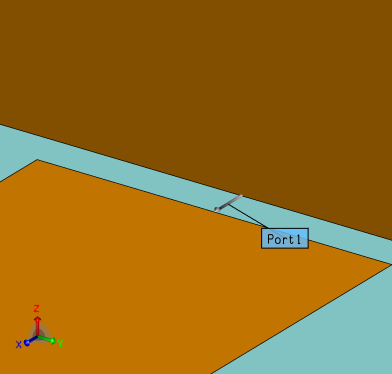
Add two FEM line ports, one for each feed line.
Tip: From the Source/Load tab select FEM line port, use the option Specify port as an edge and click on the feed line in the 3D view.

Figure 1. Zoomed in 3D view of one of the FEM line ports.