Creating the Model
Create the model in CADFEKO. Define any ports and sources required for the model. Specify the operating frequency or frequency range for the model.
- Set the model unit to millimetres.
-
Define the following variables.
- d1 = 2.22 (Distance between apertures.)
- d2 = 12.51 (Distance between apertures.)
- epsr = 2.2 (The relative permittivity of the substrate.)
- s = 10 (Length of the aperture.)
- w = 4.6 (Width of the microstrip.)
- strip_feed_arc_radius = 2*s (The radius of curved microstrip line.)
- strip_length = 2* s + d2 + d1 (The straight section length of the microstrip line.)
- substrate_depth = 50 (The substrate depth.)
- substrate_height = 1.58 (The substrate height.)
- substrate_width = 140 (The substrate width.)
- f_max = 5e9 (The maximum frequency.)
- f_min = 2.5e9 (The minimum frequency.)
-
Create a dielectric medium.
- Dielectric loss tangent: 0
- Relative permittivity: epsr
- Label: substrate
-
Create the straight section of the microstrip line.
-
Create a rectangle.
- Definition method: Base corner, width, depth
- Base corner (C): (0, -w/2, substrate_height)
- Width (W): strip_length
- Depth (D): w
-
Create a rectangle.
-
Create the feed section of the microstrip.
-
Create a rectangle.
- Definition method: Base corner, width, depth
- Base corner (C): (0, 0, 0)
- Width (W): w
- Depth (D): substrate_height
- On the Workplane tab set the Origin: (strip_length+strip_feed_arc_radius-w/2, strip_feed_arc_radius, 0)
- Rotate the workplane of the rectangle 90° around the U axis to align the rectangle in the XZ plane.
-
Create a rectangle.
-
Create the arc section of the microstrip.
-
Create an ellipse.
- Centre point (C): (strip_length, strip_feed_arc_radius, substrate_height)
- Radius (U): strip_feed_arc_radius + w/2
- Radius (V): strip_feed_arc_radius + w/2
- Label: outer_circle
-
Create a second ellipse.
- Centre point (C): (strip_length, strip_feed_arc_radius, substrate_height)
- Radius (U): strip_feed_arc_radius-w/2
- Radius (V): strip_feed_arc_radius-w/2
- Label: inner_circle
-
Subtract the inner_circle from
outer_circle.
Note: A full 360° circular microstrip section should now be visible in the 3D view. Only a section of this part will be used.
-
Create an ellipse.
- Union all parts.
-
Use face selection to remove the redundant curved face that does not form part
of the microstrip bend.
The microstrip should consist of a straight section, an arced section and a feed.
-
Simplify the remaining microstrip geometry to remove any unwanted edges.
Tip: Either select the part and click on simplify, or use edge selection and delete the redundant edge.The resulting geometry represents half of the top microstrip section.
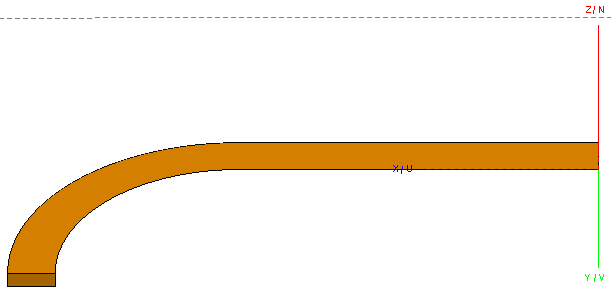
Figure 1. Geometry remaining after removing the redundant entities. -
Copy and rotate the part by 180° around the U axis.
Note: The new part represents half of the bottom microstrip.
-
Create the ground plate.
-
Create a rectangle.
- Base Corner (C): (0, -substrate_depth/2, 0)
- Width (W): substrate_width/2
- Depth (D): substrate_depth
- Label: ground_plate
-
Create a rectangle.
-
Create an aperture.
-
Create a rectangle.
- Base corner (C): (d2/2, -s/2, 0)
- Width (W):s
- Depth (D):s
- Label: aperture_1
-
Create a rectangle.
-
Create a second aperture.
-
Create a rectangle.
- Base corner (C): (d2/2+s+d1, -s/2, 0)
- Width (W):s
- Depth (D):s
- Label: aperture_2
-
Create a rectangle.
-
Subtract aperture_1 and
aperture_2 from ground_plate.
The resulting geometry is a ground plane between two microstrip lines containing two square holes.
-
Copy and mirror all geometry around the VN plane.
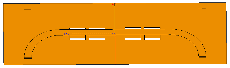
Figure 2. Geometry after the copy and mirror operation. - Union all the parts.
-
Set all faces to perfect electric conductor (PEC).
Tip: Set the faces to PEC to ensure they remain PEC when becoming faces of a dielectric region.
-
Add edge ports.
- Port1
- Define an edge port between the bottom microstrip feed on the negative X side and the ground plate.
- Port2
- Define an edge port between the bottom microstrip feed on the positive X side and the ground plate.
- Port3
- Define an edge port between the top microstrip feed on the negative X side and the ground plate.
- Port4
- Define an edge port between the top microstrip feed on the positive X side and the ground plate.
-
Create two substrate layers.
-
Create a cuboid to construct the top layer.
- Definition method: Base centre, width, depth, height
- Base centre (C): (0, 0, 0)
- Width (W): substrate_width
- Depth (D): substrate_depth
- Height (H): substrate_height
- Label: top_layer
-
Create a second cuboid to construct the bottom layer.
- Definition method: Base centre, width, depth, height
- Base centre (C): (0, 0, -substrate_height)
- Width (W): substrate_width
- Depth (D): substrate_depth
- Height (H): substrate_height
- Label: bottom_layer
- Union top_layer and bottom_layer.
- Set both regions for this Union to the dielectric, substrate.
-
Create a cuboid to construct the top layer.
- Union all the parts in the model.
-
Activate the FDTD solver.
Tip: Open the Solver settings dialog and click the FDTD tab. Select the Activate the finite difference time domain (FDTD) solver check box.
-
Set the frequency.
- Linearly spaced discrete points
- Start frequency (Hz): f_min
- End frequency (Hz): f_max
- Number of frequencies: 101