SK Card
This card defines a skin effect, ohmic losses or an arbitrary user defined impedance boundary condition on wire segments and surface elements. Layered dielectrics can also be defined.
In the Home tab, in the Define group, click
the ![]() Media icon. From
the drop-down list select the
Media icon. From
the drop-down list select the ![]() Losses (SK) icon.
Losses (SK) icon.
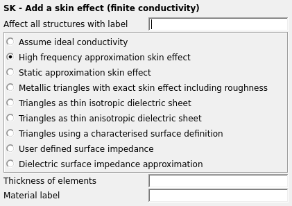
Figure 1. The SK - Add a skin effect (finite conductivity) dialog.
Parameters:
- Affect all structures with label
- The label to which the skin effect is applied is specified. All mesh elements with this label are assigned the skin effect.
- Assume ideal conductivity
- Ideal conductivity is assumed as if no SK card is specified for this label. All other parameters are ignored.
- High frequency approximation skin effect
- High frequency approximation.
- Static approximation skin effect
- Static (ohmic losses) approximation.
- Metallic triangles with exact skin effect including roughness
- Use the exact expression of the skin effect for wires and/or surfaces that is valid at arbitrary frequencies and includes the effects of surface roughness.
- Triangles as thin isotropic dielectric sheet
- Treat metallic triangles as thin isotropic dielectric layers (possibly consisting of multiple layers). Specify the label of the layered dielectric (as defined in the DL card) to be used as the medium for the thin isotropic dielectric layers.
- Triangles as thin anisotropic dielectric sheet
- Treat metallic triangles as thin anisotropic dielectric layers (possibly consisting of multiple layers). Specify the label of the layered dielectric (as defined in the DL card) to be used as the medium for the thin anisotropic dielectric layers.
- Triangles using a characterised surface definition
- Treat triangles as a characterised surface (a surface defined by transmission and reflection coefficient data). Specify the label of the characterised surface (as defined in the DI card) to be used as the medium for the characterised surface.
- User defined surface impedance
- An arbitrary user defined complex surface impedance (as defined in the DI card) can be used by specifying the label of the surface impedance.
- Thickness of elements
- The thickness d of the surface elements in metres (if an SF card is present, this is always scaled).
- Characterised surface label
- Label of the characterised surface (as specified in the DI card).
- Material label
- Label of the material which will be used (as specified in the DI card).
- Layered dielectric label
- Label of the layered dielectric medium which will be used (as specified in the DL card).
Recommendations for choosing the label(s)
It is not recommended to set the same label for both triangles and segments with Affect all structures with label. Separate labels and a unique SK card for each label should be used. In addition all wires with the label Affect all structures with label must have the same radius. If this is not the case a unique label must be created for each radius.Note: The skin depth is given by
, where the radial frequency is
and the permeability is
.