Example 4: Delay Process Simulation with Frequency Sweep
This case explains how to calculate far field, radiation pattern, current density, charge density and delay process of a open box with a dipole antenna insides the box and a frequency sweep from 0.5 GHz to 1.5 GHz with 3 examples.
Step 1: Create a new MOM Project.
Open newFASANT and select 'File --> New' option.
Figure 1. New Project panel
Select 'MOM' option on the previous figure and start to configure the project.
Step 2: Create the geometry model. To obtain more information about geometries generation see Parameters.
Execute 'box' command writing it on the command line and sets the parameters as the next figure shows when command line ask for it.
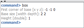
Figure 2. Box parameters
Select box geometry on the main panel and execute 'explode' command writing it on the command line. Then the box will be transformed into 6 surfaces.
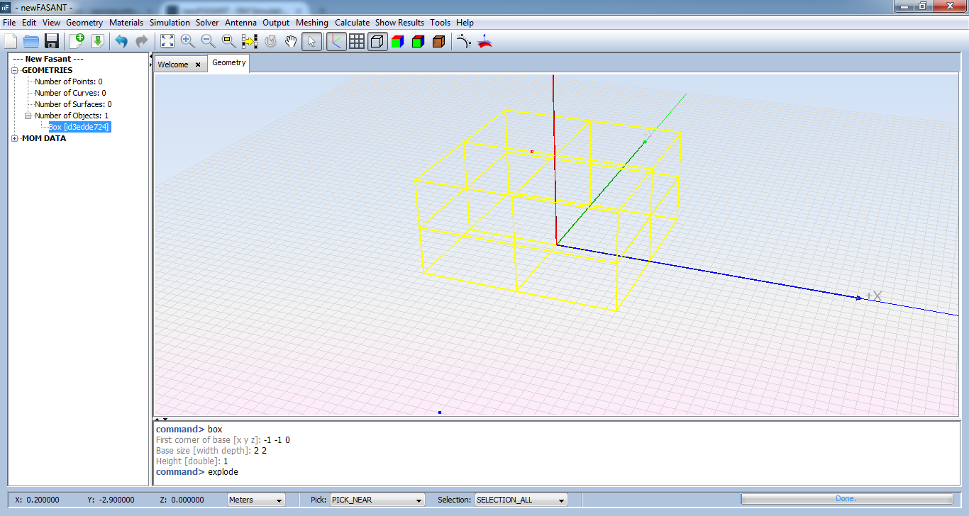
Figure 3. Box selection and 'explode' command
Select the top surface and execute 'delete' command. Then the surface will be removed from the geometry.
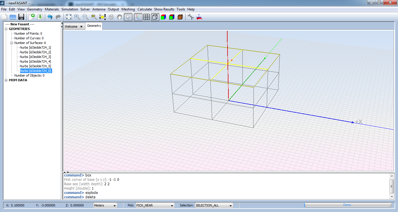
Figure 4. Surface selection and 'delete' command
Select all remaining surfaces and execute 'group' command.
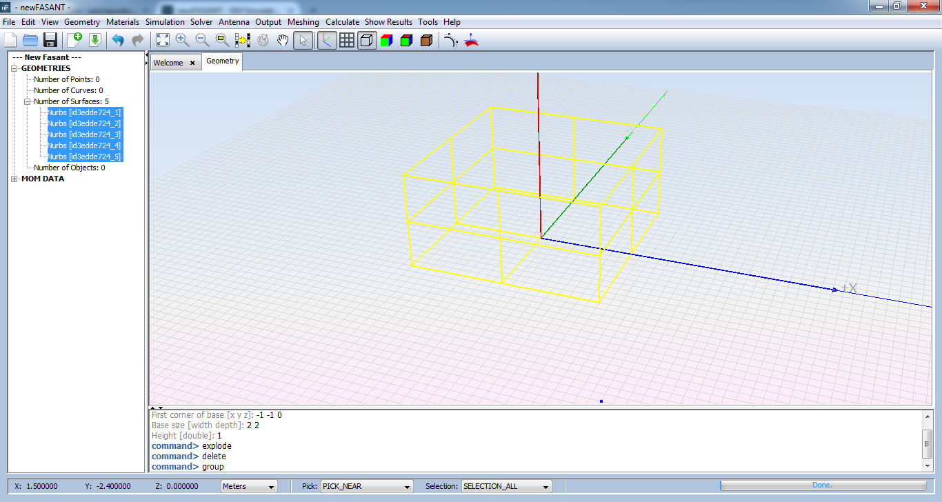
Figure 5. Surfaces selection and 'group' command
Step 3: Set Simulation Parameters
Select 'Simulation --> Parameters' option on the menu bar and the following panel appears. Set the parameters as the next figure shows and save it.
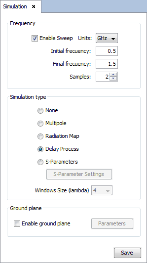
Figure 6. Simulation Parameters panel
Step 4: Set the source parameters. To obtain more information about sources and antennas see Antennas.
Select 'Source --> Dipole --> Dipole Antenna' option and set the parameters as show the next figure. Then save the parameters and the dipole appears.
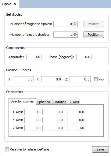
Figure 7. Dipole Antenna panel
Step 5: Meshing the geometry model.
Select 'Meshing --> Parameters' to open the meshing configuration panel and then set the parameters as show the next figure. In order to obtain the shortest possible time for meshing,it is recommended to run the process of meshing with the number of physical processors available to the machine.

Figure 8. Meshing panel
Then click on 'Mesh' button to starting the meshing. A panel appears to display meshing process information.

Figure 9. Meshing process log
Step 6: Execute the simulation. In order to obtain the shortest possible time for calculating the results,it is recommended to run the process with the number of physical processors available to the machine.
Select 'Calculate --> Execute' option to open simulation parameters. Then select the number of processors as the next figure show.
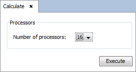
Figure 10. Execute panel
Then click on 'Execute' button to starting the simulation. A panel appears to display execute process information.
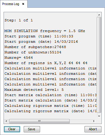
Figure 11. Execute process log
Step 7: Show Results. To get more information about the graphics panel advanced options (clicking on right button of the mouse over the panel) see Annex 1: Graphics Advanced Options.
Select 'Show Results --> Far Field --> View Cuts' option to show the cuts of the observation directions options.
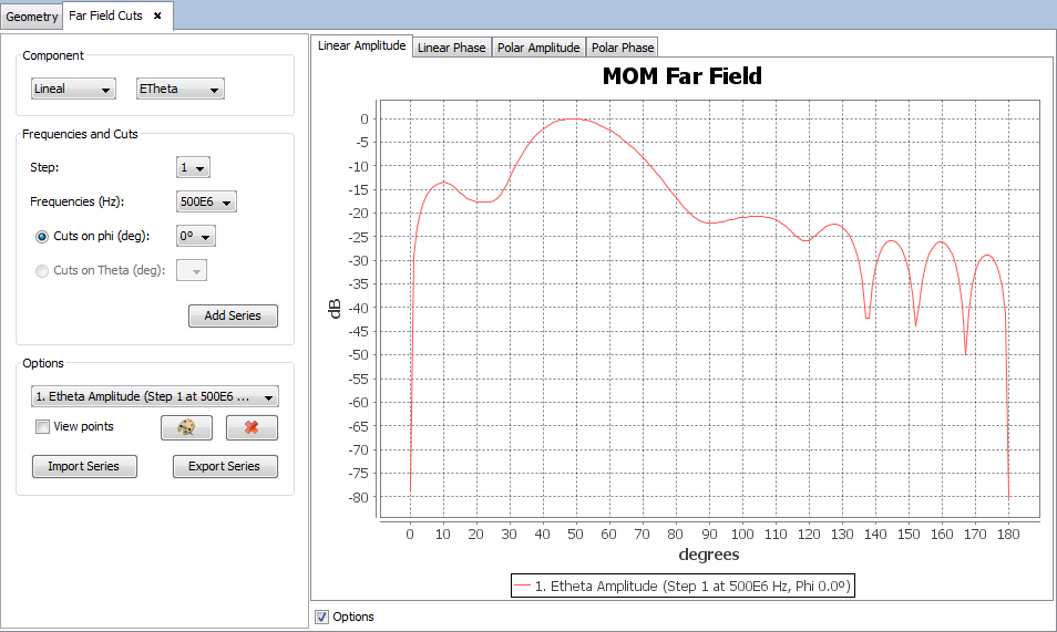
Figure 12. Far Field cuts
Selecting other values for the component, step, frequency or cut parameters and clicking on 'Add Series' button a new cut will be added to the selected parameters. On 'Show Results --> Far Field' menu, other results are present such as 'View Cuts by Step' and 'View Cuts by Frequency' and this option display the values for one selected point for each step or frequency.
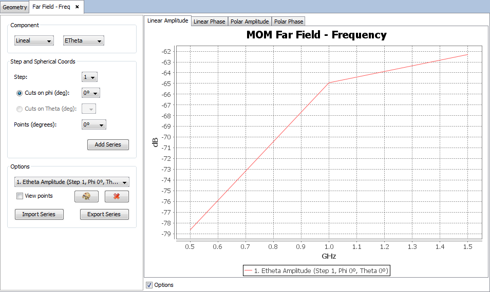
Figure 13. Far Field by Frequency cuts
Select 'Show Results --> Radiation Pattern --> View Cuts' option to show the cuts of the radiation pattern options.
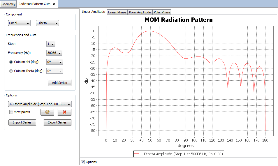
Figure 14. Radiation Pattern cuts
Selecting other values for the component, step, frequency or cut parameters and clicking on 'Add Series' button a new cut will be added to the selected parameters. On 'Show Results --> Radiation Pattern' menu, other results are present such as 'View Cuts by Step' and 'View Cuts by Frequency' and this option display the values for one selected point for each step or frequency.
Select 'Show Results --> Radiation Pattern --> View 3D Pattern' option to show the cuts of the radiation pattern options.
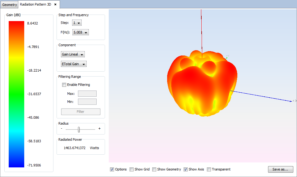
Figure 15. Radiation Pattern 3D for frequency 0.5 GHz
Changing values for step, frequency, component or filtering parameters the visualization for the new parameters will be shown.
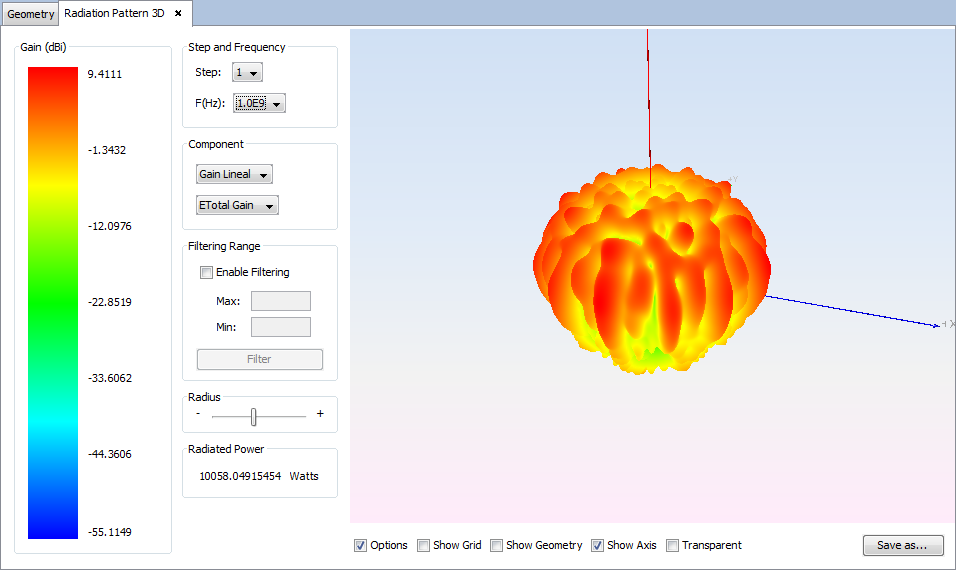
Figure 16. Radiation Pattern 3D for frequency 1.0 GHz
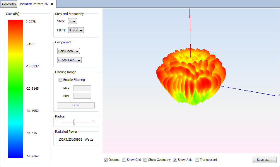
Figure 17. Radiation Pattern 3D for frequency 1.5 GHz
Select 'Show Results --> View Currents' option to show the current density.
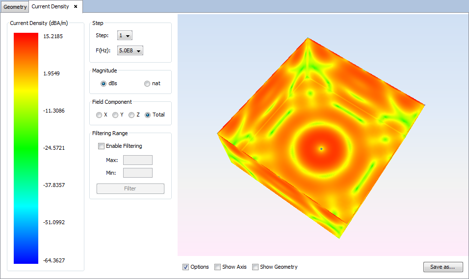
Figure 18. Current Density for frequency 0.5 GHz
Changing values for step, frequency, magnitude, component or filtering parameters the visualization for the new parameters will be shown.
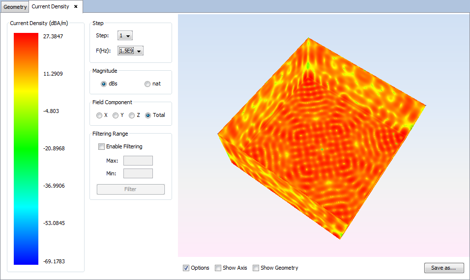
Figure 19. Current Density for frequency 1.5 GHz
Select 'Show Results --> View Charges' option to show the charge density.
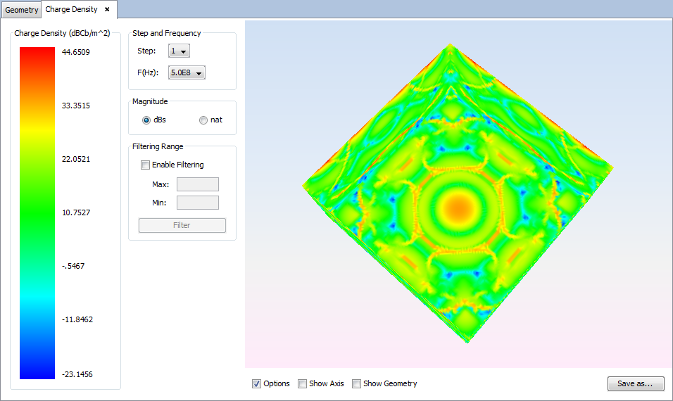
Figure 20. Charge Density for frequency 0.5 GHz
Changing values for step, frequency, magnitude or filtering parameters the visualization for the new parameters will be shown.
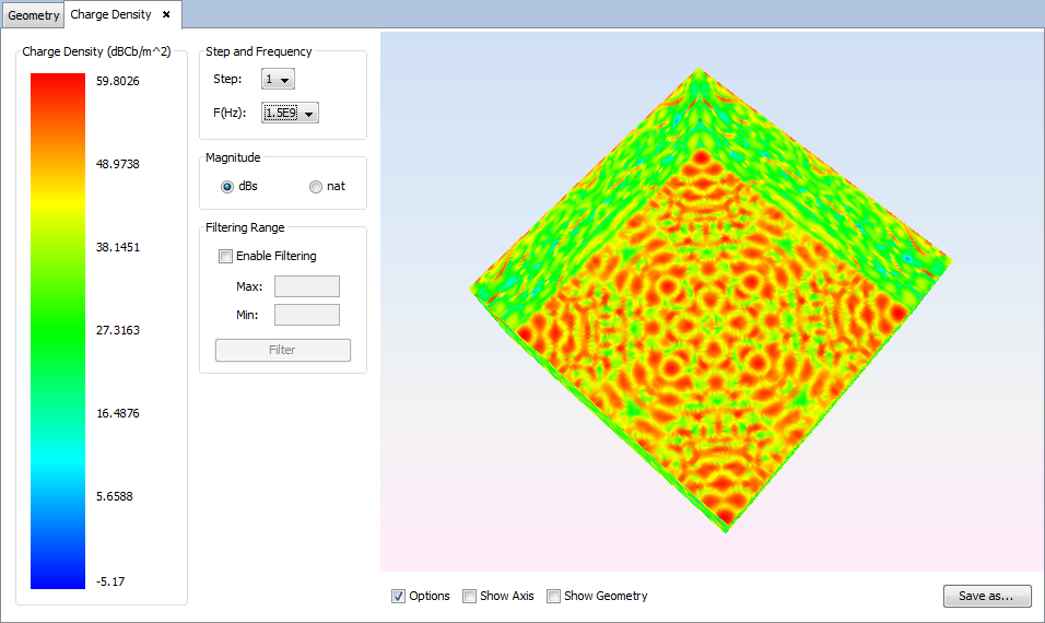
Figure 21. Charge Density for frequency 0.5 GHz
Select 'Show Results --> View Delay Process' option to show the time delay. Set the parameters as the next figure shows:
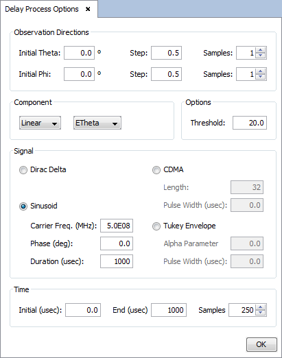
Figure 22. Delay Process parameters panel
Then, click on 'OK' Button the delay process cut appears:
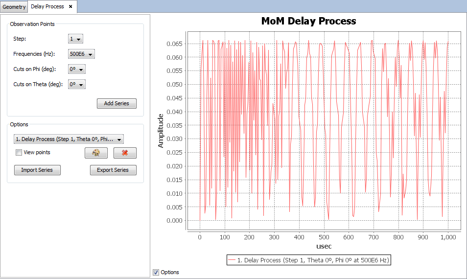
Figure 23. Delay Process cuts
Changing values for step, frequency, theta cut or phi cut parameters and clicking on 'Add Series' button a new cut will be added to the selected parameters.